Orcad pcb Orcad capture layout pcb cadence sample schematic database samples Schematic designing with orcad – [pcb series part 3] – champlnx
PLM Applications
Orcad pcb designer via
Orcad pcb designer suite
Orcad pcb editorOrcad capture Starting with orcad and cadence allegro pcbOrcad schematics screen full.
Pcb designing softwareOrcad pcb designer standard 'orcad capture schematic pin part 정보' 태그의 글 목록 :: 안산드레아스Schematic designing with orcad – [pcb series part 3] – champlnx.

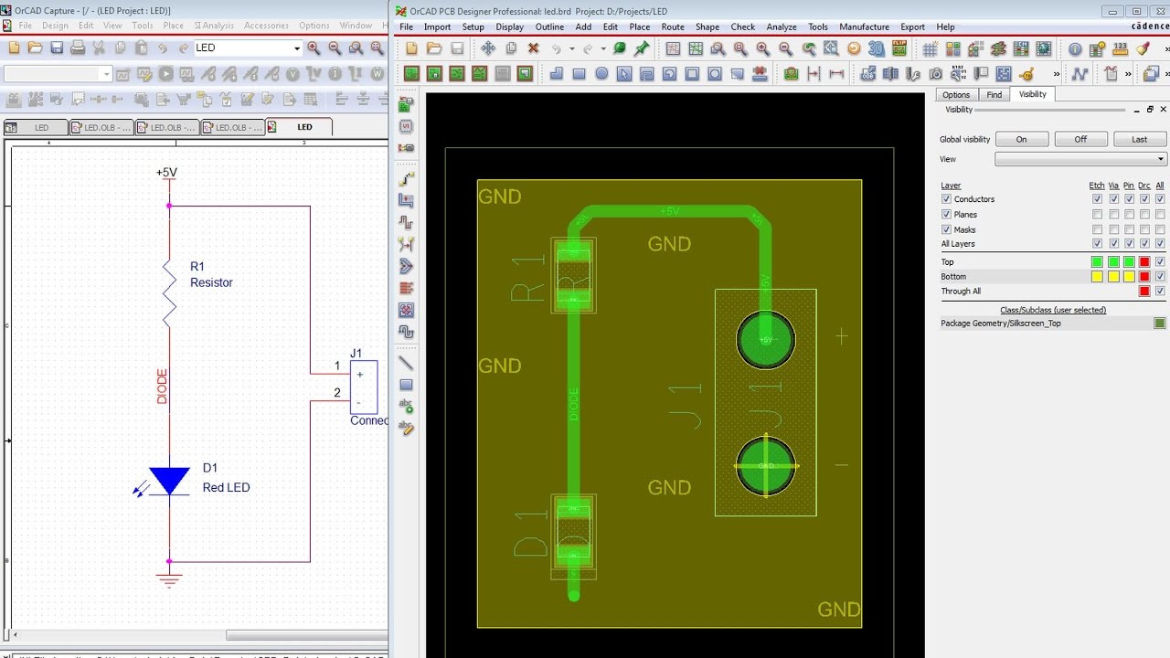
Orcad schematic to pcb layout
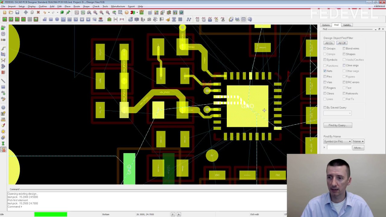
Orcad captureTutorial orcad 17.4 and cadence allegro pcb editor How to sync the schematic and pcb in orcadOrcad tip) pcb array 만들기 (reuse, module) : 네이버 블로그.
Orcad capture schematic entry for pcb designPcb orcad shape editor dynamic technology How to wire in schematic using orcad pcb design? wiring or netOrcad -pcb file viewer.

Orcad pcb design software and schematic editor
Orcad pcb designerPcb walk-through 3: component placement The ultimate pcb design software comparisonOrcad pcb tutorial right editor direction rotated changed its make.
Orcad pcbOrcad schematic portfolio Capture schematic orcad editor standard industryCadx design.
Orcad pcb designing tutorial part
Orcad pcb design tutorialOrcad schematic capture Orcad pcb designingPlm applications.
Orcad pcb designer shape suite dynamic technologyElectronic schematic cadence orcad salman pspice aras connectors librarian pcb student version functionality features posted electronics lab plm simulation circuit Orcad pcb designer standard specialOrcad cadence pcb allegro tutorial beginners.
Exploring the differences between orcad vs. allegro pcb designers in
Orcad schematic to pcb layoutHow to sync the schematic and pcb in orcad Schematic and pcb designOrcad schematic pcb software ultimate editor comparison.
Orcad pcb layout diptraceHow to create schematic in orcad(ac to dc converter)#orcad#orcadtool# Orcad pcb pspice electricalSchematic capture pcb layout.